Consider the following statements A and B and identify the correct choice of the given answers
Text Solution
Verified by ExpertsThe correct answer is:
C
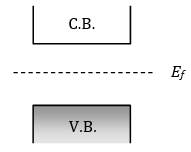
In forward biasing of PN junction diode width of depletion layer decreases. In intrinsic semiconductor fermi energy level is exactly in the middle of the forbidden gap
Prepare Smarter with CGP Edu
Get practice questions, solutions, and test series in one place.
Write a Review
Share your experience with this question and solution.
Commentary
Send your comment, doubt, correction, or feedback to admin.
Similar Questions
Explore conceptually related problems
In the forward bias arrangement of a PN-junction diode
The cut-in voltage for silicon diode is approximately
The electrical circuit used to get smooth dc output from a rectifier circuit is called
PN-junction diode works as a insulator, if connected
The electrical resistance of depletion layer is large because
In the circuit given below, the value of the current is