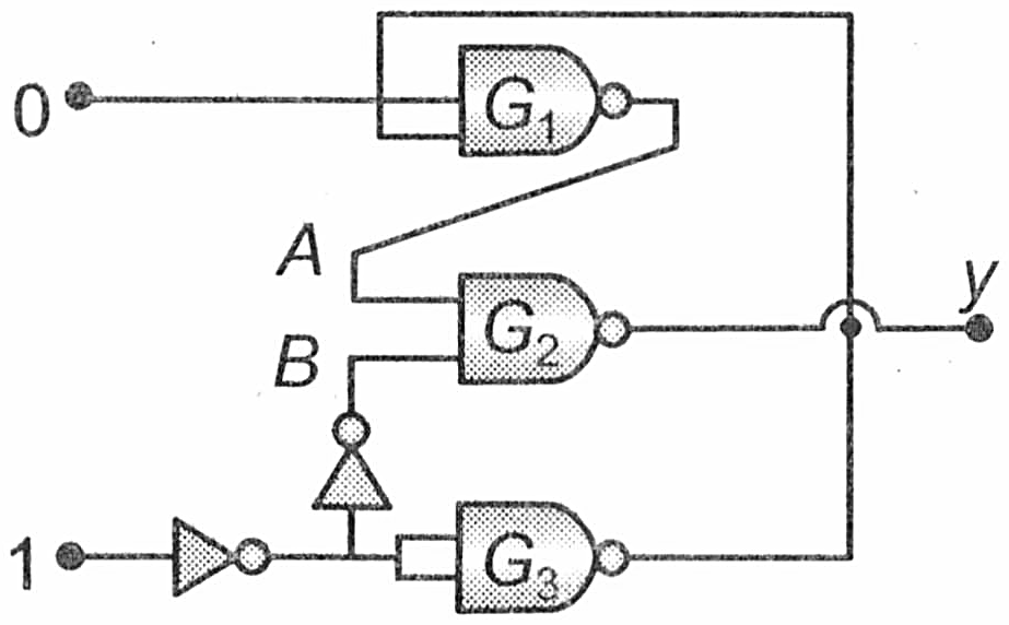
In circuit in the following figure the value of Y is
A
0
B
1
C
Fluctuates between  and 1
and 1
and 1
D
Indeterminate as the circuit can’t be realized
Text Solution
Verified by ExpertsThe correct answer is:
A
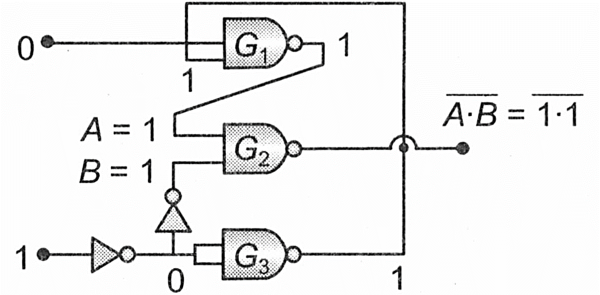
Lower NOT gate inverts input to zero. NOT gate from NAND gate inverts this output to 1 upper NAND gate converts this input 1 and input  to 1.
to 1.
Thus  and
and  become inputs of NAND gate giving final output as zero.
Prepare Smarter with CGP Edu
Get practice questions, solutions, and test series in one place.
Write a Review
Share your experience with this question and solution.
Commentary
Send your comment, doubt, correction, or feedback to admin.
Similar Questions
Explore conceptually related problems
Which represents NAND gate
The impurity atom added to germanium to make it N‐type semiconductor is
The phase difference between input and output voltages of a CE circuit is
The potential barrier developed in the diode of figure is 0.5 V. The current in the diode is curren…
When N‐type of semiconductor is heated
The width of forbidden gap in silicon crystal is 1.1 When the crystal is converted into a ‐type s…