Published by:
CGP EDU Academic Team
Published on: September 12, 2026
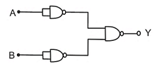
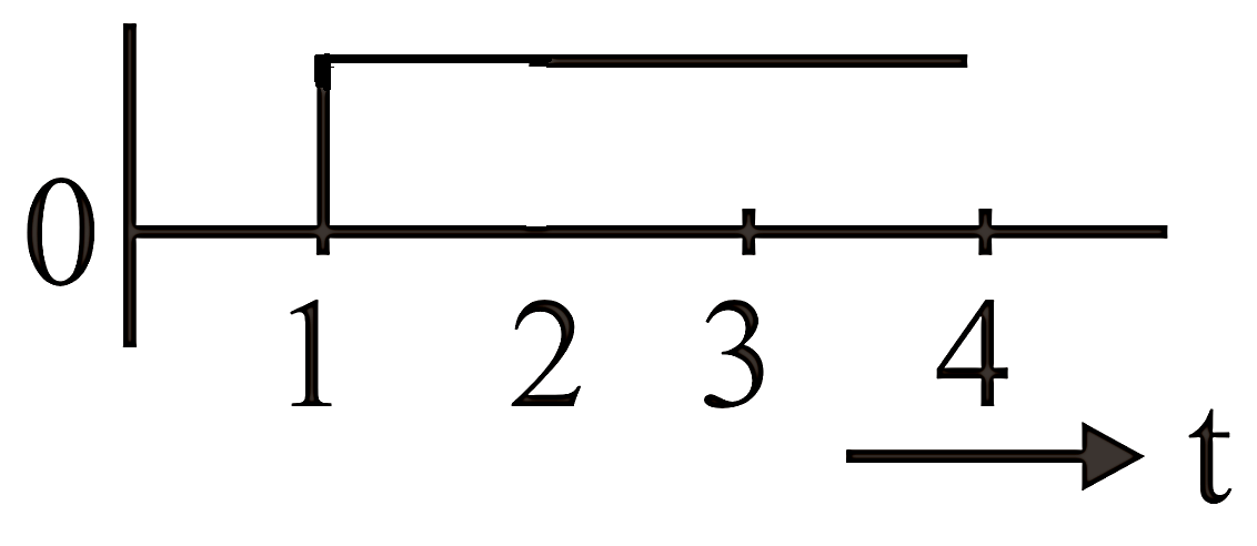
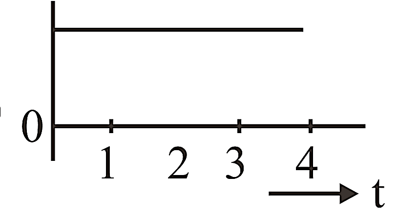
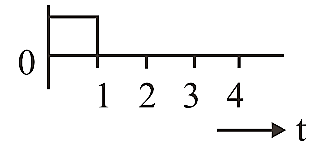
For the logic circuit shown, the output waveform at Y is
A
B
C
D
Text Solution
Verified by ExpertsThe correct answer is:
A
All the gates used in the diagram represent NAND gates.
Thus, the output Y can be calculated as follows


= A + B
The above equation suggests that the output of the given combination yields the same result as an OR gate.
The truth table can be written as follows
A | B | |||
0 | 0 | 1 | 1 | 0 |
0 | 1 | 1 | 0 | 1 |
1 | 0 | 0 | 1 | 1 |
1 | 1 | 0 | 0 | 1 |


Hence, this is the correct output.
Prepare Smarter with CGP Edu
Get practice questions, solutions, and test series in one place.
Write a Review
Share your experience with this question and solution.
Commentary
Send your comment, doubt, correction, or feedback to admin.
Similar Questions
Explore conceptually related problems
Identify the correct Logic Gate for the following output (Y) of two inputs A and B.
A logic gate circuit has two inputs A and B and output Y. The voltage waveforms of A, B and Y are s…
If and are the input voltages (either 5V or 0V) and is the output voltage then the two gates rep…
The following figure shows a logic gate circuit with two inputs and and the output . The voltage…
Which of the following logic gate is represented by the combination of logic gates?
Consider the following logic circuit.
The output is when: